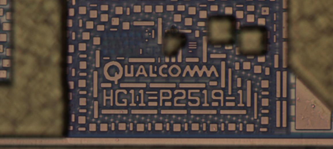
This report presents a partial circuit analysis of a selected phase locked loop (PLL) block on the Qualcomm MSM8998 SoC. Four similar PLL blocks and one different PLL block can be seen on the MSM8998 die, all with visible spiral inductors and recognizable PLL layout features. The Qualcomm MSM8998 SoC die is manufactured in Samsung 13-metal, single-poly,10nm LPE FinFET process. An added thin film resistor layer is found on the metal 1 layer. The die size is measured 7.84mm by 9.22mm, given an area of 72.30mm² which is a little bit smaller than Apple A11.
This report consists of the hierarchically-organized transistor-level circuit function analysis of the selected PLL block, presented in both pdf format for general review and IC Explorer for crossing circuit-layout review. The IC Explorer outputs industry formats of netlists including SPICE, Verilog, VHDL, and EDIF200 for function verification and performance simulations.
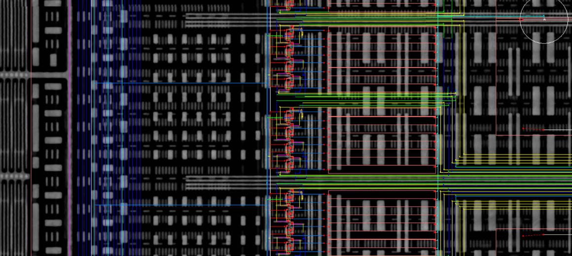
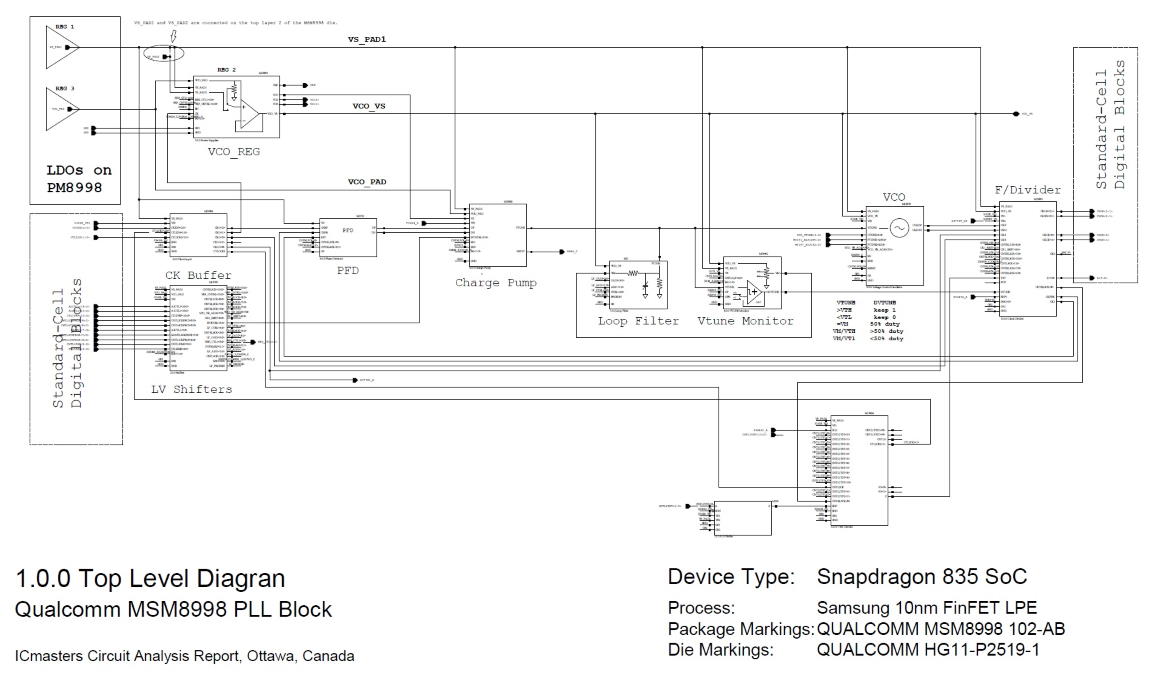
Schematic 1.0.0 shows the top level diagram of the PLL block of the Qualcomm MSM8998 SoC. The partially analyzed PLL circuits are organized in twelve subcircuits: 2.0.0 CKF Input, 3.0.0 Phase Detector, 4.0.0 Charge Pump, 5.0.0 VCO with LC Tank, 6.0.0 Loop Filter, 7.0.0 Regulator VCO, 8.0.0 Frequency Divider, 9.0.0 Clock Output, 10.0.0 Timer, 11.0.0 Comparator and 12.0.0 Current Generator. The PLL block is located on the I/O area of the Qualcomm MSM8998 SoC die as shown on Page 8 of this report.
The schematic 2.0.0 CKF Input is a buffering circuit for reference input. The digital phase detector in Schematic 3.0.0 is a dual D-type flip flop phase comparator. Delay buffers are used in the reset feedback loop to prevent the dead zone.
The charge pump circuit in Schematic 4.1.0 is connected to two programmable current resources. Schematic 12.0.0 shows one of the programmable current resources which includes a large number of current generator cells (Schematic 12.1.0 and Schematic 12.2.0). A comparator is used for monitoring the charge pump voltage range. An LDO voltage regulator (Schematic 7.2.0) is used to generate a smooth programmable power supply for the LC tank VCO… Unlock the full report
The report includes the full design review.
1.0.0 Top Level Diagram
2.0.0 CKF Input
3.0.0 Phase Detector
4.0.0 Charge Pump
5.0.0 VCO with LC Tank
6.0.0 Loop Filter
7.0.0 Regulator VCO
8.0.0 Frequency Divider
9.0.0 Clock Output
10.0.0 Timer
11.0.0 Comparator
12.0.0 Current Generator
Digital Cell Library
The report includes the interactive schematic and layout image database at high-resolution.
Hierarchically organized schematics and high-resolution layout images
Report delivered with interactive software
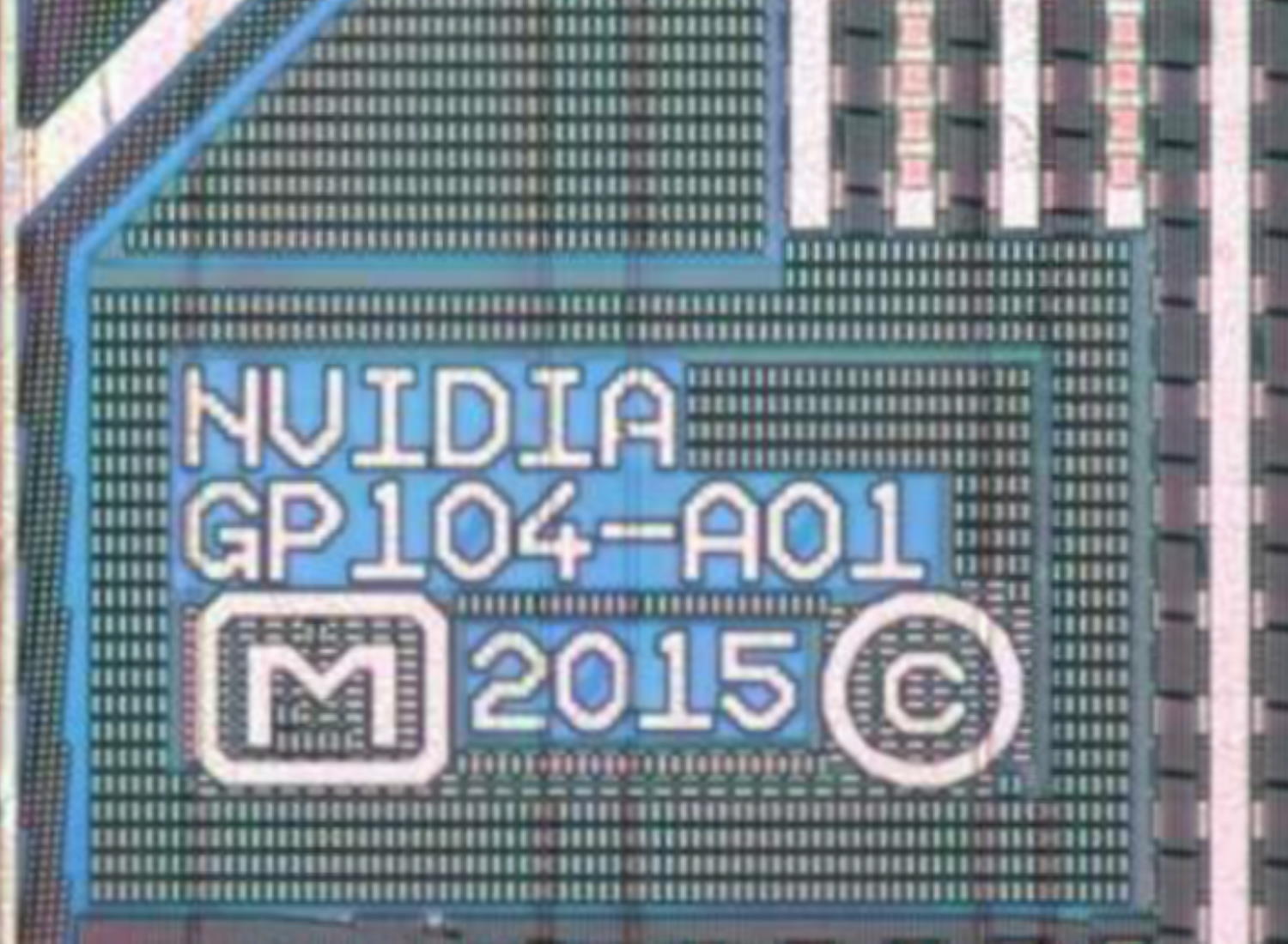
Die markings: NVIDIA GP104-A01 2015
| Apple |
| Qualcomm |
| Sandisk |
| Microsoft |
| Samsung |
| AMD |
| IBM |
| Mellanox |
| Micron |
| Mitsubishi |
| Bosch |
| STMicroelectronics |
| Maxim |
| Nintendo |
| MediaTek |
| Xilinx |
| Macronix |
| Powerchip |
| General Motors |
| Sony |
| NVIDIA |
| NVIDIA GP104 (GeForce GT1070) GPU |
| Mellanox Ethernet Switch |
| Sandisk USB Memory |
| Mitsubishi RF Device |
| STMicroelectronics IIS328DQ 3-axis Accelerometer |
| Microsoft XBOX ONE CPU |
| MediaTek Helio P20 (MT6757) |
| Qualcomm PMIC |
| IBM Processor |
| Macronix XtraROM |
| Samsung 3D NAND SRAM |
| Xilinx Virtex 2 Pro |
| AMD Athlon 3200+ CPU |
| Qualcomm WCN3990 2×2 802.11ac Wifi |
| Powerchip NAND |
| Bosch BMI055 Inertial Sensor |
| Micron DDR4 DRAM |
| Nintendo ROM |
| Qualcomm MSM8992 Snapdragon 808 SoC |
| Bosch BMI260 Inertial Sensor |
| Qualcomm MSM8998 Snapdragon 835 APU |
| General Motors Sensor Module |
| Apple A11 APU |
| Sony CMOS Image Sensor |
| Bosch BMI160 Inertial Sensor |
| STMicroelectronics ISM330DLC Inertial Sensor |
| STMicroelectronics CMOS Image Sensor |
| Bosch BMA280 Accelerometer |
| MediaTek X20 (MT6797W) APU |
| Xillinx Spartan 3 |
| Non-Infringement Analysis |
| Planar imaging of SRAM cells |
| Layout analysis |
| Package and bevel layout analysis |
| Circuit schematic extraction |
| Brief die analysis |
| Circuit patent evidence of use |
| Patent Categorization |
| Board tracing |
| Brief die analysis |
| Custom circuit simulation |
| Patent Reviews |
| Package cross-section analysis |
| Process structure |
| Process patent evidence of use |
| Package layout high resolution imaging |
| Package, die photo, delayering |
| Sensor module analysis |
| Prior Use Analysis |
| GPIO block |
| GDDR5X interface circuit |
| RF Power Amplifier (PA) |
| Inertial sensor circuits and structures |
| OLED modules |
| CIS column comparator circuit |
| Temperature sensors and control circuits |
| GPU layout |
| Dummy metals in SRAM interconnect |
| VCO |
| 6T and 8T SRAM |
| RF devices |
| GPU charge pump circuit |
| Level 2 Cache SRAM |
| PMIC |
| GPU comparator circuit |
| CIS layout analysis |
| Phase-Lock-Loop (PLL) |