NVIDIA GP104 GPU (GeForce GT1070)

Circuit Analysis Report

An I/O Pad of GDDR5X Interface​


Images from the report

This report presents a partial circuit analysis of a selected repeating I/O pads on a GDDR5X interface of the GP104 GPU. The GP104 GPU die is made in TSMC 14-metal, 16nm FinFET process with a die size of 19.3mm by 16.4mm.This report consists of the circuit analysis of the selected GDDR5X data I/O pad, organized hierarchically in transistor-level. The report is presented in both pdf format for general review and IC Explorer for crossing circuitlayout review. The IC Explorer can output industry formats of netlists including SPICE, Verilog, VHDL, and EDIF200 for function verification and performance simulations.

From the report’s design overview:

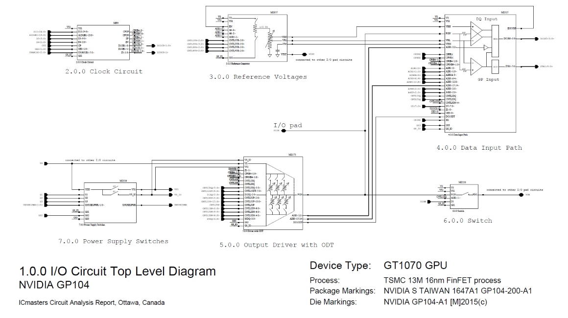
Schematic 1.0.0 shows the top level diagram of the selected GDDR5X high speed DQ I/O circuit on the NVIDIA GP104 GPU die. The partially analyzed circuits are organized in seven subcircuits: Schematic 2.0.0 Clock Circuit, Schematic 3.0.0 Reference Generator, Schematic 4.0.0 Data Input Path, Schematic 5.0.0 Driver with ODT, Schematic 6.0.0 Switch and Schematic 7.0.0 Power Supply Switches.

The schematic 2.0.0 shows clock generating circuits of this DQ I/O pad. Two pairs of processed clock signals are sent to the Schematic 4.0.0 Data Input Path and Schematic 5.0.0 Driver with ODT. An additional pair of processed clock signals are send to the unanalyzed standard-cell digital area that is not far away from the clock generating block.

The Reference Generator in Schematic 3.0.0 is a high accuracy resistor ladder which generates a pair of precise voltages VRH/VRL for data input circuits as references… Unlock the full report

The report includes the full design review.

The report includes interactive schematics for the following subcircuits:

1.0.0 Top Level Diagram
2.0.0 Clock Circuit
3.0.0 Reference Generator
4.0.0 Data Input Path,
5.0.0 Driver with ODT
6.0.0 Switch
7.0.0 Power Supply Switches

The report includes the interactive schematic and layout image database at high-resolution.

Also check out our Qualcomm report:

Qualcomm Snapdragon 835 APU

PLL Block Circuit Analysis Report
10nm FinFET process in Samsung LPE Technology


Hierarchically organized schematics and high-resolution layout images
Report delivered with interactive software
Package markings: Qualcomm MSM8998 102-AB
Die markings: Qualcomm HG11-P2519-1

Other reports and analysis

Apple
Qualcomm
Sandisk
Microsoft
Samsung
AMD
IBM
Mellanox
Micron
Mitsubishi
Bosch
STMicroelectronics
Maxim
Nintendo
MediaTek
Xilinx
Macronix
Powerchip
General Motors
Sony
NVIDIA
NVIDIA GP104 (GeForce GT1070) GPU
Mellanox Ethernet Switch
Sandisk USB Memory
Mitsubishi RF Device
STMicroelectronics IIS328DQ 3-axis Accelerometer
Microsoft XBOX ONE CPU
MediaTek Helio P20 (MT6757)
Qualcomm PMIC
IBM Processor
Macronix XtraROM
Samsung 3D NAND SRAM
Xilinx Virtex 2 Pro
AMD Athlon 3200+ CPU
Qualcomm WCN3990 2×2 802.11ac Wifi
Powerchip NAND
Bosch BMI055 Inertial Sensor
Micron DDR4 DRAM
Nintendo ROM
Qualcomm MSM8992 Snapdragon 808 SoC
Bosch BMI260 Inertial Sensor
Qualcomm MSM8998 Snapdragon 835 APU
General Motors Sensor Module
Apple A11 APU
Sony CMOS Image Sensor
Bosch BMI160 Inertial Sensor
STMicroelectronics ISM330DLC Inertial Sensor
STMicroelectronics CMOS Image Sensor
Bosch BMA280 Accelerometer
MediaTek X20 (MT6797W) APU
Xillinx Spartan 3
Non-Infringement Analysis
Planar imaging of SRAM cells
Layout analysis
Package and bevel layout analysis
Circuit schematic extraction
Brief die analysis
Circuit patent evidence of use
Patent Categorization
Board tracing
Brief die analysis
Custom circuit simulation
Patent Reviews
Package cross-section analysis
Process structure
Process patent evidence of use
Package layout high resolution imaging
Package, die photo, delayering
Sensor module analysis
Prior Use Analysis
GPIO block
GDDR5X interface circuit
RF Power Amplifier (PA)
Inertial sensor circuits and structures
OLED modules
CIS column comparator circuit
Temperature sensors and control circuits
GPU layout
Dummy metals in SRAM interconnect
VCO
6T and 8T SRAM
RF devices
GPU charge pump circuit
Level 2 Cache SRAM
PMIC
GPU comparator circuit
CIS layout analysis
Phase-Lock-Loop (PLL)

Report enquiries can be submitted below:

    tripadvisor flickr americanexpress bandcamp basecamp behance bigcartel bitbucket blogger codepen compropago digg dribbble dropbox ello etsy eventbrite evernote facebook feedly github gitlab goodreads googleplus instagram kickstarter lastfm line linkedin mailchimp mastercard medium meetup messenger mixcloud paypal periscope pinterest quora reddit rss runkeeper shopify signal sinaweibo skype slack snapchat soundcloud sourceforge spotify stackoverflow stripe stumbleupon trello tumblr twitch twitter uber vimeo vine visa vsco wechat whatsapp wheniwork wordpress xero xing yelp youtube zerply zillow px aboutme airbnb amazon pencil envelope bubble magnifier cross menu arrow-up arrow-down arrow-left arrow-right envelope-o caret-down caret-up caret-left caret-right